
What the study found
The study reports a 12-bit, 10 MS/s two-step sub-ranging successive approximation register (SAR) analog-to-digital converter (ADC) with top-plate dividing. The authors say this design reduces capacitance, avoids gain and offset mismatches between coarse and fine conversions, and achieves competitive performance and energy efficiency.
Why the authors say this matters
The authors state that dividing the top-plate sampling node enables residue amplification within a single-stage SAR ADC, avoiding the need for a multi-stage design. They also suggest that eliminating gain and offset mismatches improves robustness and linearity.
What the researchers tested
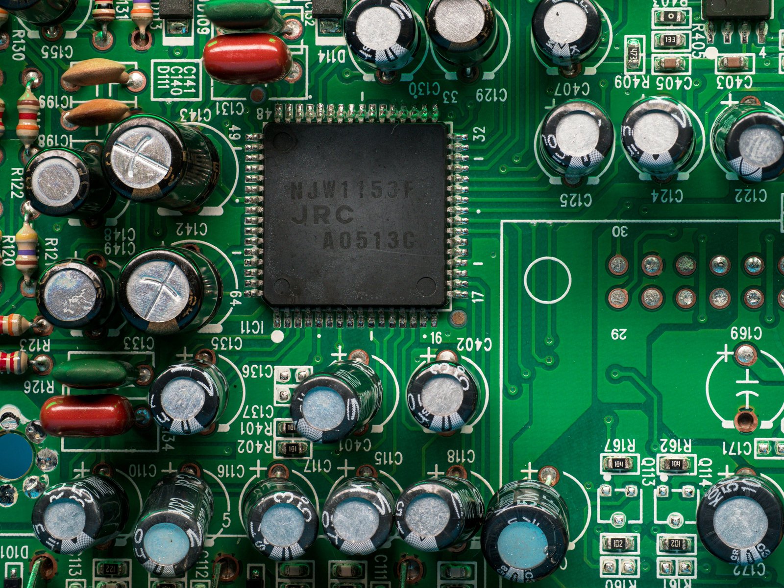
The researchers proposed and fabricated a prototype ADC in a 65 nm CMOS process. The design uses a two-step sub-ranging SAR architecture with top-plate dividing and an analog residue amplifier.
What worked and what didn't
The prototype occupies 252 μm × 227 μm and achieves an SNDR of 65.7 dB at Nyquist-rate input. The total CDAC capacitance is reduced by 86% compared with a conventional SAR ADC with the same unit-capacitor size, and the residue amplifier drives one-fourth of the total CDAC capacitance. The chip consumes 227.7 μW from a 1.2 V supply and has a Walden FoM of 14.5 fJ/conversion step.
What to keep in mind
The abstract does not describe detailed limitations or comparisons beyond the stated CDAC-capacitance reduction and performance figures. The summary available here is limited to the information provided in the title and abstract.
Key points
- A 12-bit, 10 MS/s two-step sub-ranging SAR ADC with top-plate dividing is proposed.
- The design reduces CDAC capacitance by 86% versus a conventional SAR ADC with the same unit-capacitor size.
- The residue amplifier drives one-fourth of the total CDAC capacitance.
- The fabricated 65 nm CMOS prototype achieves 65.7 dB SNDR at Nyquist-rate input.
- The chip consumes 227.7 μW at 1.2 V and has a Walden FoM of 14.5 fJ/conversion step.
Disclosure
- Research title:
- Two-step SAR ADC cuts capacitance and stays energy efficient
- Authors:
- Jaegeun Song, Chaegang Lim
- Institutions:
- Hankuk University of Foreign Studies, Samsung (South Korea)
- Publication date:
- 2026-03-03
- OpenAlex record:
- View
Get the weekly research newsletter
Stay current with peer-reviewed research without reading academic papers — one filtered digest, every Friday.